(Singapore)

Product Summary
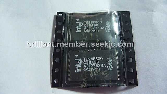
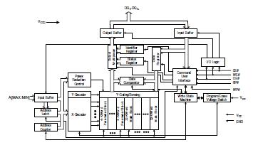
The TE28F800C3BA is an Advanced Boot Block Flash Memory. The TE28F800C3BA provides high-performance asynchronous reads in package-compatible densities with a 16 bit data bus. Individually-erasable memory blocks are optimally sized for code and data storage. Eight 4 Kword parameter blocks are located in the boot block at either the top or bottom of the device’s memory map. The rest of the memory array is grouped into 32 Kword main blocks. The TE28F800C3BA supports read-array mode operations at various I/O voltages (1.8 V and 3 V) and erase and program operations at 3 V or 12 V VPP. With the 3 V I/O option, VCC and VPP can be tied together for a simple, ultra-low-power design. In addition to I/O voltage flexibility, the dedicated VPP input provides complete data protection when VPP ≤ VPPLK.
Parametrics
TE28F800C3BA absolute maximum ratings: (1)During Read: -40℃ to +85℃; (2)During Block Erase and Program: -40℃ to +85℃; (3)Temperature under Bias: -40℃ to +85℃; (4)Storage Temperature: -65℃ to +125℃; (5)Voltage On Any Pin (except VCC and VPP) with Respect to GND: -0.5 V to +3.7 V; (6)VPP Voltage (for Block Erase and Program) with Respect to: GND -0.5 V to +13.5 V; (7)VCC and VCCQ Supply Voltage with Respect to GND: -0.2 V to +3.6 V; (8)Output Short Circuit Current: 100 mA.
Features
TE28F800C3BA features: (1)Flexible SmartVoltage Technology, 2.7 V. 3.6 V Read/Program/Erase; 12 V for Fast Production Programming; (2)1.65 V.2.5 V or 2.7 V.3.6 V I/O Option, Reduces Overall System Power; (3)High Performance, 2.7 V. 3.6 V: 70 ns Max Access Time; (4)Optimized Architecture for Code Plus Data Storage, Eight 4 Kword Blocks, Top or Bottom Parameter Boot; Up to One Hundred-Twenty-Seven 32 Kword Blocks; Fast Program Suspend Capability; Fast Erase Suspend Capability; (5)Flexible Block Locking, Lock/Unlock Any Block; Full Protection on Power-Up; WP# Pin for Hardware Block Protection; (6)Low Power Consumption, 9 mA Typical Read; 7 A Typical Standby with Automatic Power Savings Feature (APS); (7)Extended Temperature Operation, -40℃ to +85℃; (8)128-bit Protection Register, 64 bit Unique Device Identifier; 64 bit User Programmable OTP Cells; (9)Extended Cycling Capability, Minimum 100,000 Block Erase Cycles; (10)Software, IntelR Flash Data Integrator (FDI); Supports Top or Bottom Boot Storage, Streaming Data (e.g., voice); Intel Basic Command Set; Common Flash Interface (CFI); (11)Standard Surface Mount Packaging, 48-Ball μBGA/VFBGA; 64-Ball Easy BGA Packages; 48-Lead TSOP Package; (12)ETOX.VIII (0.13 μm) Flash Technology, 16, 32 Mbit; (13)ETOX.VII (0.18 μm) Flash Technology, 16, 32, 64 Mbit; (14)ETOX.VI (0.25 μm) Flash Technology, 8, 16 and 32 Mbit.
Diagrams
 |
 TE28F004S3-150 |
Other |
|
Data Sheet |
Negotiable |
|
||||
|
TE28F004S5-100 |
Other |
|
Data Sheet |
Negotiable |
|
||||
|
TE28F004SC-100 |
Other |
|
Data Sheet |
Negotiable |
|
||||
|
TE28F008B3B120 |
Other |
|
Data Sheet |
Negotiable |
|
||||
|
TE28F008B3BA110 |
Other |
|
Data Sheet |
Negotiable |
|
||||
|
TE28F008SA-100 |
Other |
|
Data Sheet |
Negotiable |
|
||||